     |
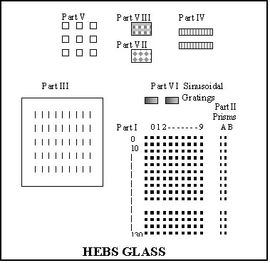
The mask pattern is written with an e-beam writer with a 0.1 mm addressing grid size and consists of the following eight parts.
Part I: This part helps users to match photoresist heights with specific optical densities (OD, or D herein after) in the mask to build a calibration curve "height of photoresist after development vs. OD of mask pattern." Part I exhibits 140 gray levels that are identified with labels, ranging from 0 to 139. Each gray level consists of one test patch, each test patch being 100µm x 100µm in size. The gray levels are designated optical density values according to the equation D = 0.126 + 0.010101i, where i = 0, 1, 2 . . . 139. Thus, by using the equation, the minimum and maximum OD can be determined to be 0.126 and 1.53004, respectively. In general, the heights of resist thickness remaining will level off at an OD value between 0.8 to 1.2, because of the limited dynamic range of an analog photoresist. (Please see the CMI info sheet, "Photoresist Analog Transfer Scheme for HEBS-Glass Photomasks".) Because most photoresists have a limited dynamic range and respond to about 1 unit of OD value--for example, from 0.12 to 1.12, HEBS-Glass Plate HEBS5 with an e-beam sensitized glass layer of 1 micrometer is designed to satisfy this OD range. HEBS-Glass masks with a larger OD range can be useful for other applications such as for use with certain photopolymers and other photoresists. HEBS-Glass Calibration Plate I85 B provides test patterns and test strips having OD values up to 2.0. HEBS-Glass Plates I85 having an e-beam sensitized glass layer of 3 micron is capable of OD values up to 4.0 using an e-beam accelerating voltage of 30KV or higher. Although there may be only 100 calibrated OD levels within the dynamic range of a photoresist, mask patterns having more than 500 gray levels can be written in a HEBS-Glass Plate reproducibly. Any arbitrary value of OD in the OD range of 0.126 to 1.53004 can be produced in HEBS-Glass Plate HEBS5. There exists no universal calibration curve that is valid for all users. Height of photoresist after development may be a linear or a monotonic nonlinear function of transmittance of a mask pattern, or maybe a linear or a monotonic nonlinear function of OD of a mask pattern. The variable parameters governing the calibration curve include the variable parameters of photolithography tools such as exposure wavelength and intensity, and the variable parameters of photoresists and development including the type of photoresist and the as-coated thickness of photoresist. Nevertheless, when as coated photoresist thickness is very thin such as less than 1 micrometer, it is likely that the height of photoresist after development is a linear function of the transmittance (T here in after) of the mask pattern.
Part II: Part II labeled "Prisms" consists of tapered structures of variable heights for applications such as micro-prisms and micro-mirrors, each facet may have a unique compound tilt. Column A are prisms with a constant D T and column B are prisms with a constant D OD between adjacent gray levels. Each 100m mx100m m prism has 50 gray levels. The formula for the transmittance values of column A is Ti=Tmax-[(Tmax-Tmin)/49]i where i = 0, 1, 2, 3, 4…,49. The formula for the OD values of column B is ODi=ODmin + [(ODmax – ODmin)/49]i, where i = 0, 1, 2, 3, 4,…,49. The OD ranges and the corresponding transmittance ranges for the prisms in both column A and B are as follows:
|
| Company | Technology | Products | Online Help | Contact |