|
The Photoresist Analog Transfer Scheme for HEBS-Glass Photomasks
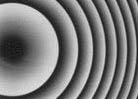
Analog surface height profile in photoresist from a single optical
lithographic
exposure using one HEBS-glass gray level mask
Introduction
Photoresists designed for IC fabrication are binary photoresists. Due to the existence of
a threshhold effect, binary microstructures are produced with conventional photolithographic
processes using all types of photomasks including chrome masks. To create binary structures
in photoresist, it is necessary that the optical density (OD) of chrome is more than 1.2.
When the OD of the mask is much below 1.2, even with the binary photoresist, there exists a
dynamic range where the developed resist thickness is a function of the optical density of
the photomask. This dynamic range can be extended by the analog transfer scheme described
below. The dynamic range of photoresist in the analog transfer scheme, in general,
cooresponds to OD values in the range of 0.1 to 0.85. The dynamic range of a positive
non-chemically amplified, Novalac-based photoresist can, in general, be extended to about
1.0 in OD value.
The Procedure of Processing Photoresist to Produce an Analog Resist Profile
-
Clean substrate (e.g. quartz plates)
with heated resist stripper.
-
Rinse thoroughly with Di water.
-
Dry out bake at about 120oC
for 1 hour.
-
Allow to cool down and spin a layer of OeBR-514
(photoresist from Olin Ciba Geigy) at 2500 rpm for 30 seconds. This should give a
layer slightly above 1 micron thickness.
-
Softbake photoresist at a low temperature and for
a shortened time from that which is normally used for binary lithography. For OeBr-514
use 90oC in a convection oven for 15 minutes instead of the recommended 30
minutes. This increases the sensitivity and will also make the contrast curve more linear
and increase the dynamic range of the analog transfer scheme.
-
After exposure for a batch development with low
agitation (move plate once every 5 seconds e.g. lift half an inch, slowly move down),
use a standard Metal-Ion-Free developer which is rather weak and has lower contrast
compared to the usual developers, e.g. Shipley MF-319.
-
Immediately follow with a Di water rinse.
Be very careful not to spray or force any features away.
-
Postbake for several hours in a 90oC oven.
Higher temperatures will melt the features in the resist.
(Note: the above procedure was developed
for Olin Ciba Geigy’s OeBR-514 resist which is no longer available for
purchase. Please see below for available photoresists.)
-
In principle, other resists can be used in a
similar way. Just adjust the processing temperature or duration to reduce the
heat schedules for softbake. Specifically, use a bake duration that is a factor
of 0.5 to 0.67 of the manufacturer's recommendations for binary lithography
(e.g. 15 to 20 minutes instead of 30 minutes). The photoresist should be a positive
and non-chemically amplified, Novolac-based photoresist.
-
Other photoresists that have also been used
successfully are: Shipley STR1045, STR 1075 and S1650, and Clariant AZ P4620,
AZ P4330-RS and AZ 4562.
-
Resist features having thickness range from
submicron up to more than 20 micron were produced with HEBS glass masks having
gray levels in the OD range of 0.1 to 1.2.
|