


|
||
|
Canyon Materials, Inc. (CMI) specializes in the fabrication of true grayscale ( i.e. not halftone ) photomasks for use in grayscale photolithography to produce 3-D microstructures. E-beam written HEBS-glass photomasks and laser beam written LDW-glass photomasks are all-glass photomasks having no chrome or any other coating on the all-glass mask surface. Customers' designed 3D microstructures are manufactured using an all-glass gray scale photomask wherein a gray scale pattern having 2 to 1000 gray levels, is written with an electron beam (e-beam) or a laser beam pattern generator. The mask pattern is written within a surface glass layer of the all-glass photomask. Each 0.1 micron spot or line of the mask pattern is written with a pre-determined transmittance value. HEBS glass and LDW glass are patented glass products of Canyon Materials, Inc. HEBS-glass photomask blanks are the 1997 Photonic Circle of Excellence Award winner. See more about the award here. All-glass gray scale photomasks include HEBS-glass and LDW-glass masks. The all-glass gray scale photomasks which have no coating of any kind do not have any abrupt change in refractive index in the mask patterns such as those exist in chrome line edges or half tone chrome dots in the conventional chrome on glass masks. Without the undesirable scattering or diffraction, a true gray scale optical density pattern in an all-glass mask is faithfully and reproducibly converted into a corresponding gray scale height pattern in photoresist through an otherwise conventional optical lithographic process.
The all-glass gray scale photomasks enable mass fabrication of 3-D microstructures including refractive microlens arrays, diffractive optical elements (DOE), tapered structures for microelectronic and micromechanical devices, beam shaping elements, and much more. Successful optoelectronic consumer products and medical devices containing key optical elements made with the use of CMI's all-glass grayscale photomask technology have been growing in number in the world-wide market. The all-glass masks also enable fabrication of apodization filters and various grayscale transmission filters including single frequency sinusoidal gratings with zero harmonic distortion.
U.S. Patent No. 6,562,523B1 and No. 6,524,756B1 of Canyon Materials, Inc. (CMI) describe the all-glass ( i.e. HEBS-glass and LDW-glass ) grayscale photomask technology which includes the method of making an All-glass grayscale photomask and the method of making 3D micro-structures using an all-glass grayscale photomask.
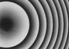
CMI's HEBS-glass and LDW-glass grayscale photomask technology have been used by U.S. and foreign companies for mass-production of high quality microlens arrays and diffractive optical elements. The yield in mass-production of micro optical elements, which mainly depends on the shape error and surface quality, is such that the all-glass grayscale photomask technology has been used in mass-production of most demanding applications. For example, with a non-exclusive license from CMI, Panasonic uses all-glass mask technology to mass-produce 9.5 mm height Ultra Slim Super Multi Drives incorporating a grayscale diffractive optic. The ALL-glass grayscale mask technology improved the signal quality of the drives by increasing the diffraction efficiency of the diffractive optic and brought significant reduction of cost per drive as a result. Consequently, the all-glass grayscale mask technology made the Panasonic optical drives very competitive in terms of technology and cost. The shape error of the diffractive optical element in the Ultra Slim Super Multi Drive is less than 10 nm. The use of gray scale optics improved the diffraction efficiency from 32% to 85%. The very high quality of microoptical elements made with the all-glass mask technology, stems from intrinsic properties of HEBS-glass and LDW-glass and is apparent by comparing mask pattern images in a HEBS-glass mask vs. those in a conventional half tone mask; please see Photos 1 and 2 of CMI Product Information No. 04-100.
For a quick look at the all-glass gray scale mask technology, please see exemplary micro-elements made using a HEBS-glass mask, and also see exemplary masks.
See additional merits of the all-glass grayscale mask technology and see how you can design your own microlens arrays and tapered structures using the all-glass gray scale mask technology by reading CMI Product Information No. 01-88 "All-Glass Gray Scale Mask Technology."
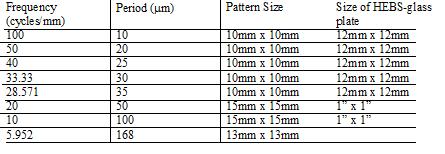
CMI has e-beam writers in-house; available write grids are 25nm (i.e. 25 nanometer), 50nm, and 100nm. For good throughput and still very high gray scale resolution, HEBS-glass gray scale masks are typically written with a pixel size of 100nm (i.e. 0.1 micron). Within a 5"x5" pattern area, each of the gray pixels may have an optical density value or a transmittance value selected from more than 500 gray levels. The number of grayscale levels in a HEBS-glass mask is only limited by the accuracy and reproducibility of the clock rates of a vector scan e-beam writer. In the data file for writing an all-glass grayscale photomask, each gray level is a layer. For example, a mask written with 100 layers of GDS data file is used to fabricate a 3D microstructure having 100 gray scale height levels. Most often, the number of gray levels is chosen being sufficiently large so that a photoresist can not resolve discrete height levels and a smooth surface profile is produced in photoresist.
HEBS-glass plates offer true gray scale photomasks with the highest gray scale resolution possible! CMI Product Information No. 04-100 describes how All-glass gray scale photomasks offer the highest gray scale resolution when compared to alternative gray scale photomask techniques like halftone masks and photographic emulsion masks.
Numerous all-glass gray scale masks (see exemplary masks) were made for a variety of applications.
Among many fabrication techniques that were used to produce microoptical elements, all-glass gray scale mask technology remains the most flexible, versatile, and accurate method. With an all-glass gray scale mask, the fabrication of microoptical elements uses conventional IC fabrication tools. Any existing model of contact aligners, projection printers, and steppers designed for IC fabrication can be used in gray scale photolithography using an all-glass gray scale photomask. Large arrays of 3D microstructures in 4", 5", 6", 8" or 12" wafers can be produced using a 1X or a 5X stepper.
All-glass gray scale photomasks enable economic mass fabrication of 3D microstructures in photoresist, in fused silica, in silicon, and in visible, near infrared and/or infrared transmitting substrates. Moreover, even for the fabrication of a mold surface for embossing or compression molding of plastic optical elements, photolithography using an all-glass grayscale photomask to make the surface profile of the mold is preferred over e-beam or laser beam direct write on photoresist, for both quality and economic advantages, see bullet points No. 1 to 4 and points 5a to 5i of CMI Product Information No. 01-88.
Ultimate Quality CGHs - Computer generated holograms (CGHs) with many phase levels are produced from an all-glass grayscale photomask in one photolithographic step. A gray pixel in a random phase plate may be 0.1 micron, or much larger pixel sizes for economic reason.
Leading Edge Microlens Fabrication - CMI's all-glass masks enable users to create traditional as well as new designs of microlens arrays: e.g. 100% fill factor with square or hexagonal aperture, aspheric or spherical lenses, each lenslet in an array can be unique, e.g. Microlenses Designed with Varied Degree of Compound Tilt.
The micro-optical elements produced with an all-glass photomask are proven particularly effective to improve efficiency of imaging, collimation, beam splitting and funneling light into an active area in each pixel of an array, including, for example, a refractive microlens array with 100% fill factor for focusing light onto the optically active part in each detector cell of a CCD or a CMOS Imager, similarly, a refractive microlens array with 100% fill factor to funnel light through the transmissive region of each TFT transistor which turns each pixel in an LCD display on and off giving brighter images, a refractive microlens array for Shack-Hartman wavefront sensor, prealigned arrays of microlenses to collimate light from fibers or from laser diode sources, and much more.
Companies using CMI's all-glass gray scale photomasks for research and/or production of 3D microelements include Panasonic Communications Co. Ltd., Panasonic Boston Laboratory, ITRI of Taiwan, Advanced Medical Optics, Wavefront Sciences Inc., Rockwell Science Center, Seiko Epson, Canon, Nikon, NASA, Sandia National Laboratories, Ricoh, Sony, NTT Communications, Dong Jin Semichem Co. Ltd., Raytheon Company, Teledyne Scientific & Imagining, LLC, De La Rue Group of U.K., Olympus, Samsung, Samsung America, Inc., Alps, Epson, SII of Japan, Yamatake, Asahi, Samsung Electronics, Co., Ltd., Smithsonian Observatory, Jet Propulsion Laboratories, Western Digital Corp., Lockheed Martin Coherent Technologies, among many others.
A HEBS-glass calibration plate is designed for use to optimize an analog resist process, and to establish resist height vs. optical density relationship, so that users of CMI's all-glass gray scale photomask can convert their design of resist height into optical density in a HEBS-glass mask or in a LDW-glass mask, and be ready to make a grayscale photomask for production use. Please see the description of HEBS-glass calibration plates. HEBS5 calibration plate is suitable for use with thinner resists of e.g. less than about 10 micron as-coated resist thickness, whereas I85P+N calibration plate is designed for use with thicker resists of eg. up 60 micron in positive photoresists, and up to 500 micron in SU8. It is worth noting that an etch ratio of 100 is obtainable for silicon vs. resist. Selectivities in the range of 80 to 100 generally work for AZ series, Shipley 18xx series, and SPR resists which are some of the most commonly used resists for MEMS processing. See Photoresist Analog Transfer Scheme for HEBS-glass Photomasks for some suggestions on how to use a commercially available binary resist for an analog resist process.
|
||
|
Company | Technology | Products | Online Help | Contact | ||